Проектирование и оптимизация аналого-цифрового флеш преобразователя c использованием дополнительных транзисторов ожидания с логикой управления током
DOI:
https://doi.org/10.20535/S0021347013100026Ключові слова:
мощность утечки, ASTCML, аналого-цифровой флеш преобразователь, АЦПАнотація
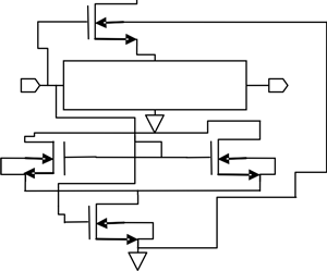
Представлена оптимизация аналого-цифрового флеш преобразователя с целью уменьшения тока утечки и вносимой задержки, используя дополнительные транзисторы ожидания с логикой управления током ASTCML (Augmented Sleep Transistors with Current Mode Logic) в 45 нм технологическом процессе. Как показали исследования, мощность утечки при использовании ASTCML уменьшается на 50% при напряжении питания 1 В. Благодаря уменьшению тока утечки снижается вероятность термической утечки, что повышает надежность устройства, хотя рассматриваемый аналого-цифровой преобразователь спроектирован на базе PMOS и NMOS. Предлагаемый аналого-цифровой преобразователь пригоден для использования в высокоскоростных и беспроводных сетевых приложениях. В работе рассмотрены различные варианты использования аналого-цифрового флеш преобразователя.
Посилання
- Sethuram R. Leakage power profiling and leakage power reduction using DFT hardware / R. Sethuram, K. Arabi, M. Abu-Rahma // 29th IEEE VLSI Test Symposium (VTS) : 1–5 May 2011, Dana Point, CA. — 2011. — P. 46–51. — DOI : http://dx.doi.org/10.1109/VTS.2011.5783753">10.1109/VTS.2011.5783753.
- Khouri K. S. Leakage power analysis and reduction during behavioral synthesis / K. S. Khouri, N. K. Jha // IEEE Trans. Very Large Scale Integration (VLSI) Systems. — Dec. 2002. — Vol. 10, No. 6. — P. 876–885. — DOI : http://dx.doi.org/10.1109/TVLSI.2002.808436">10.1109/TVLSI.2002.808436.
- Halter J. P. A gate-level leakage power reduction method for ultra-low-power CMOS circuits / J. P. Halter and F. N. Najm // IEEE Custom Integrated Circuits Conf. : CICC, 5–8 May 1997, Santa Clara, CA : proc. of conf. — 1997. — P. 475–478. — DOI : http://dx.doi.org/10.1109/CICC.1997.606670">10.1109/CICC.1997.606670.
- Tuan T. Leakage power analysis of a 90nm FPGA / T. Tuan and B. Lai // IEEE Custom Integrated Circuits Conf. : CICC, 21-24 Sept. 2003. — 2003. — P. 57–60. — DOI : http://dx.doi.org/10.1109/CICC.2003.1249359">10.1109/CICC.2003.1249359.
- Chun J. W. A novel leakage power reduction technique for CMOS circuit design / Jae Woong Chun, C. Y. R. Chen // SoC Design Conf. : ISOCC, 22-23 Nov. 2010, Seoul. — 2010. — P. 119–122. — DOI : http://dx.doi.org/10.1109/SOCDC.2010.5682957">10.1109/SOCDC.2010.5682957.
- Jalan A. Analysis of leakage power reduction techniques in digital circuits / A. Jalan and M. Khosla // Annual IEEE India Conf. : INDICON, 16–18 Dec. 2011, Hyderabad. — 2011. — P. 1–4. — DOI : http://dx.doi.org/10.1109/INDCON.2011.6139374">10.1109/INDCON.2011.6139374.
- Yeap G. Practical Low Power Digital VLSI Design / Gary Yeap. — Kluwer Academic Publishers, 1998.
- Li L. CMOS current mode logic gates for high-speed applications / Lisha Li, Sripriya Raghavendran, Donald T. Comer // 12th NASA Symp. on VLSI Design : Oct. 4–5, 2005, Coeur d’Alene, Idaho, USA. — 2005.
- Allam M. W. Dynamic current mode logic (DyCML): A new low-power high-performance logic style / Mohamed W. Allam and Mohamed I. Elmasry // IEEE J. Solid-State Circuits. — Mar. 2001. — Vol. 36, No. 3. — P. 550–558. — DOI : http://dx.doi.org/10.1109/4.910495">10.1109/4.910495.
- Rajani H. P. Novel sleep transistor techniques for low leakage power peripheral circuits / H. P. Rajani and Srimannarayan Kulkarni // Int. J. VLSI design & Commun. Syst. — 2012. — Vol. 3, No. 4. — DOI : http://dx.doi.org/10.5121/vlsic.2012.3408">10.5121/vlsic.2012.3408.
- Sharma V. K. Comparison among different CMOS inverter for low leakage at different technologies / Vijay Kumar Sharma and Surender Soni // Int. J. Appl. Eng. Res. Dindigul. — 2010. — Vol. 1, No. 2. — P. 228–233.
- Ghafari P. Impact of technology scaling on leakage reduction techniques / P. Ghafari, M. Anis, M. Elmasry // IEEE Northeast Workshop on Circuit and Systems : 5–8 Aug. 2007, Montreal, Que. — 2007. — P. 1405–1408. — DOI : http://dx.doi.org/10.1109/NEWCAS.2007.4488021">10.1109/NEWCAS.2007.4488021.
- Roy S. Impact of runtime leakage reduction techniques on delay and power sensitivity under effective channel length variations / S. Roy and A. Pal // IEEE Region 10 Conf. : TENCON 2008, 19–21 Nov. 2008, Hyderabad. — 2008. — P. 1–6. — DOI : http://dx.doi.org/10.1109/TENCON.2008.4766400">10.1109/TENCON.2008.4766400.
- Khandelwal V. Leakage control through fine-grained placement and sizing of sleep transistors / V. Khandelwal and A. Srivastava // IEEE Trans. CAD Integr. Circuits Syst. — July 2004. — Vol. 26, No. 7. — P. 533–536. — DOI : http://dx.doi.org/10.1109/TCAD.2006.888282">10.1109/TCAD.2006.888282.
- Rani M. J. Leakage power reduction and analysis of CMOS sequential circuits / M. Janaki Rani and S. Malarkann // Int. J. VLSI design & Commun. Syst. — 2012. — Vol. 3, No. 1. — P. 13–23. — DOI : http://dx.doi.org/10.5121/vlsic.2012.3102">10.5121/vlsic.2012.3102.
- Augsburger S. A. Combining dual-supply, dual-threshold and transistor sizing for power reduction / S. Augsburger and B. Nigolic // Computer Design: VLSI in Computers and Processors : IEEE Int. Conf. — 2002. — P. 316–321. — DOI : http://dx.doi.org/10.1109/ICCD.2002.1106788">10.1109/ICCD.2002.1106788.
- Waste N. H. E. Principles of CMOS Design: A system perspective / Neil H. E. Waste and K. Eshraghian. — 2nd ed. — Pearson Publication, Inc. and dorling Kindersley Publishing, Inc., 2000.
- Kumar D. Performance analysis of dynamic threshold MOS (DTMOS) 4-input multiplexer switch for low power and high speed FPGA design / Deepak Kumar, Pankaj Kumar, Manisha Pattanaik // Integrated Circuits and System Design : 23rd Symp. SBCCI’10, Sept. 2010. — 2010. — P. 2–7. — DOI : http://dx.doi.org/10.1145/1854153.1854156">10.1145/1854153.1854156.
- Sylvester D. Future performance challenges in nanometer design / D. Sylvester, H. Kaul // DAC 2001, June 18–22, 2001, Las Vegas, Nevada, USA. — June 2001. — P. 3–8.
- Kumar P. Design & implementation of low power 3-bit flash ADC in 0.18mm CMOS / Pradeep Kumar and Amit Kolhe // Int. J. Soft Comput. Eng. — 2011. — Vol. 1, No. 5. — P. 71–74. http://www.ijsce.org/attachments/File/Vol-1_Issue-5/E0150081511.pdf "> http://www.ijsce.org/attachments/File/Vol-1_Issue-5/E0150081511.pdf .
- Shehata K. A. Design and implementation of a high speed low power 4-bit Flash ADC / K. A. Shehata, H. F. Ragai, H. Husien // Design & Technology of Integrated Systems in Nanoscale Era : IEEE Int. Conf. DTIS, 2-5 Sept. 2007, Rabat. — 2007. — P. 200–203. — DOI : http://dx.doi.org/10.1109/DTIS.2007.4449519">10.1109/DTIS.2007.4449519.
- Al-Ibrahim M. M. A new fast analog-to-digital counting converter / M. M. Al-Ibrahim, S. Bataineh, M. Irshid // Electronics, Circuits & Systems : Third IEEE Int. Conf. ICECS’96, 13–16 Oct 1996, Rodos. — 1996. — Vol. 2. — P. 912–915. — DOI : http://dx.doi.org/10.1109/ICECS.1996.584533">10.1109/ICECS.1996.584533.
- Design of a low power, variable-resolution flash ADC / S. Veeramachanen, A. M. Kumar, V. Tummala, M. B. Srinivas // VLSI Design : 22nd Int. Conf., 5–9 Jan. 2009, New Delhi. — 2009. — P. 117–122. — DOI : http://dx.doi.org/10.1109/VLSI.Design.2009.62">10.1109/VLSI.Design.2009.62.
- Sharma V. K. Comparison among different CMOS inverter for low leakage at different technologies / Vijay Kumar Sharma and Surender Soni // Int. J. Appl. Eng. Res. Dindigul. — 2010. — Vol. 1, No. 2. http://www.ipublishing.co.in/jarvol1no12010/EIJAER1021.pdf "> http://www.ipublishing.co.in/jarvol1no12010/EIJAER1021.pdf.
- Singh A. K. Digital VLSI Design / Ajay Kumar Singh. — PHI Publication, 2011. — 368 p.
- Yoo J. A 1-GSPS CMOS flash A/D converter for system-on-chip applications / Jincheol Yoo, Kyusun Choi, Ali Tangel // IEEE Computer Society Workshop on VLSI : WVLSI ’01. — 2001. — P. 135–139.
- Richards T. C. Dynamic testing of A/D converters using the coherence function / T. C. Richards // IEEE Trans. Instrum. Meas. — Dec. 2006. — Vol. 55, No. 6. — P. 2265–2274. — DOI : http://dx.doi.org/10.1109/TIM.2006.884127">10.1109/TIM.2006.884127.